2-68L
0.5-17.5mm
0.1mm
3mil
1+n+1/ 2+n+2/ 3+n+3
3/3mil
+/-5%
12oz
18:1
650 x 1130mm
FR4/ Hi-Tg/ Rogers/ HALOGEN Free/ RCC/ PTFE/ Nelco
HASL/ HASL PB FREE/ Immersion Gold/ Tin/ Silver/ Gold Finger Plating/ OSP/ Immersion Gold + OSP
Flying Probe Test and In Circuit Test
Could be customized
General Specifications
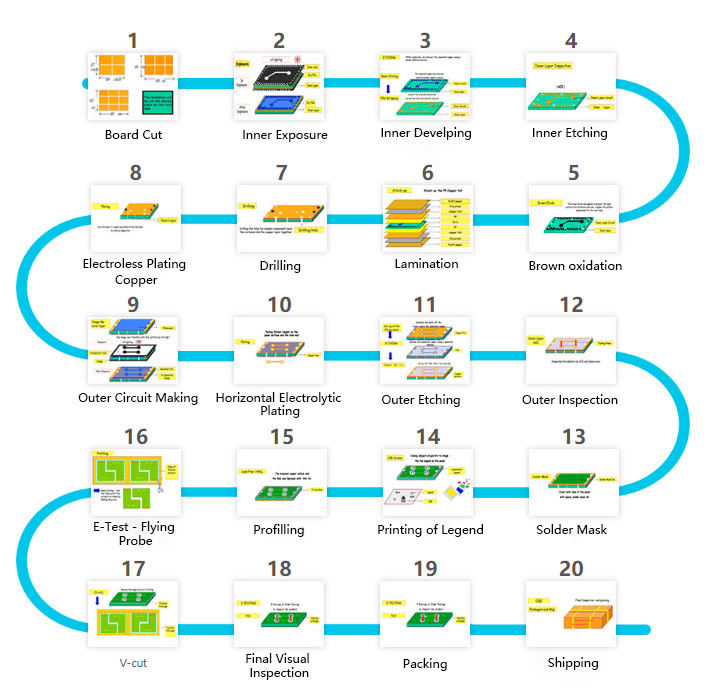
PCB Fabrication
PCB production Capabilities to meet your needs and are complied with

Layer: 2-68L
PCB Thickness: 0.5-17.5mm
Min. Mechanical Hole Dia.: 0.1mm
Min. Laser Hole Dia.: 3mil
HDI Type: 1+n+1/ 2+n+2/ 3+n+3
Min. Line/ Track Width: 3/3mil
Impedance Control: +/-5%
Max Copper Thickness: 12oz
Max Board Thickness Hole Dia. Ratio: 18:1
Max Board Size: 650 x 1130mm
PCB Material: FR4/ Hi-Tg/ Rogers/ HALOGEN Free/ RCC/ PTFE/ Nelco
Surface Treament: HASL/ HASL PB FREE/ Immersion Gold/ Tin/ Silver/ Gold Finger Plating/ OSP/ Immersion Gold + OSP
Special Process:
Testing: Flying Probe Test and In Circuit Test
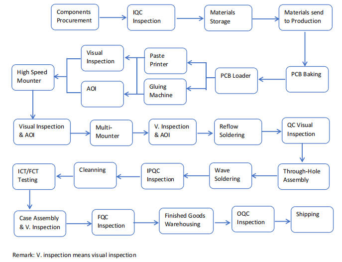
PCB Work Flow
Related Products